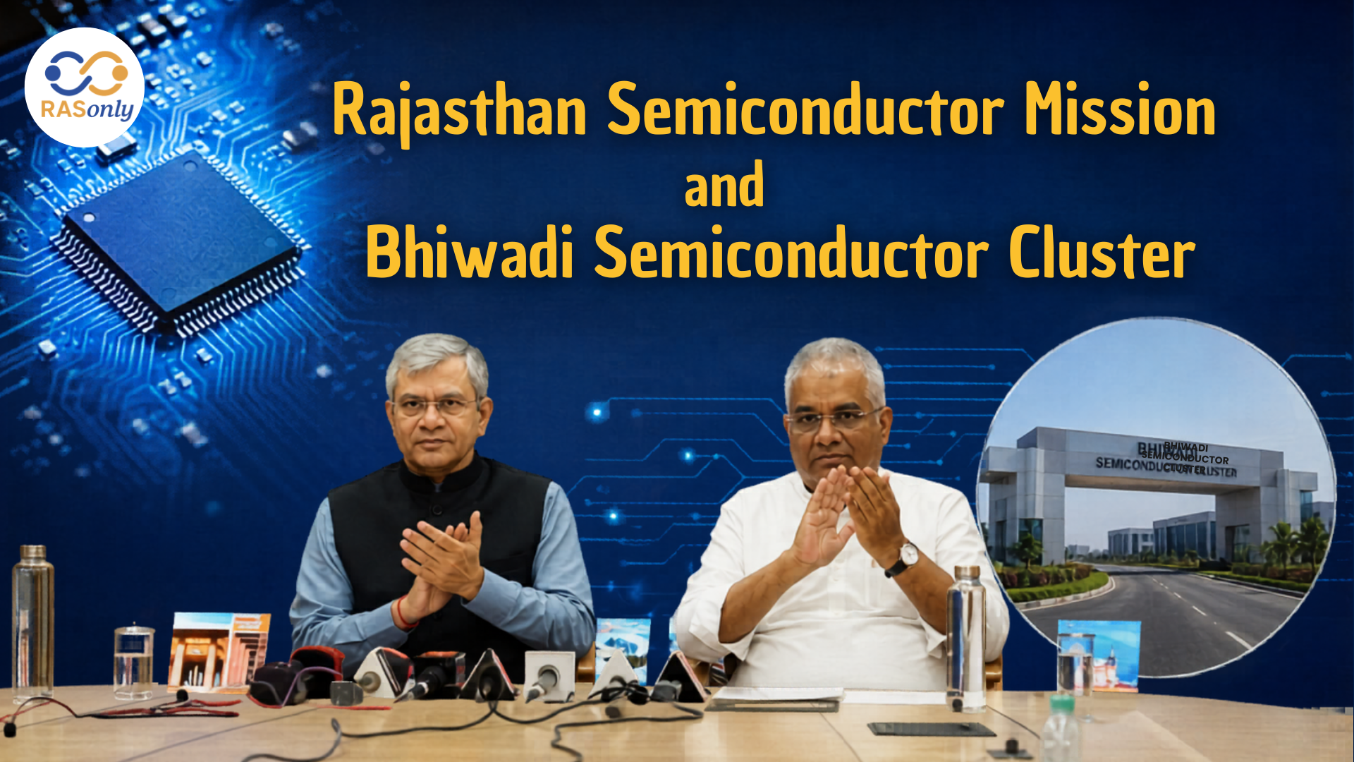
The first semiconductor cluster of the state in Bhiwadi is a giant leap towards the high-tech economy in Rajasthan. The initiative is important for the state's industrial transition, as it is a linkage between investing, advanced manufacturing, and skill development and employment creation. The cluster at Salarpur-Khushkhera in Bhiwadi has been established as a ‘Greenfield’ electronics manufacturing cluster, and is also slated to become the first SME semiconductor facility in India. As a part of the broader vision of “Viksit Rajasthan-2047”, this development will further set a strong foundation for Rajasthan's involvement in India's semiconductor mission.
The Bhiwadi semiconductor cluster has the following key features:
- The first semiconductor cluster of the state has been set up in Salarpur Khushkhera in Bhiwadi.
- It has been developed by ELCINA Electronics Manufacturing Cluster Private Limited along with 20 companies.
- It is said to be India's first SME semiconductor plant.
- There are investments proposals worth more than ₹1,200 crore received.
- 11 companies, including Sahasra Semiconductors Private Limited, Sahasra Electronics Private Limited and E-Pack Durable Limited, have started operations with an investment of ₹900 crore.
- So far, some 2,700 have been employed.
- Industries in the cluster are those that are relevant to semiconductors, electronic components, RFID, EV components, and manufacture of air conditioner components.
- At present, it has a packaging capacity of 6 crore semiconductor units per year.
- This capacity is planned to be increased to 40–60 crore units in the next 2–3 years.
- Advanced packaging technologies, SSDs, DRM and other data storage products are also in the planning phase.
Why the Semiconductor Industry Matters
Semiconductors are the foundation of today's technology. They are used in mobile phones, missiles, electric vehicles, artificial intelligence systems, electronic devices and advanced industrial machines. Till now, countries such as the USA, China, Taiwan and South Korea have dominated this sector. Thus, India's emphasis on semiconductors is crucial for technological autonomy, national security, industrial growth, and integration into the global supply chain.
India Semiconductor Mission and Rajasthan’s Role
In December 2021, India launched “India Semiconductor Mission 1.0” to boost its semiconductor capacity. The Union Budget 2026-27 has allocated ₹1,000 crore for “India Semiconductor Mission 2.0”. The objective of this mission is to not only create chip manufacturing, but also semiconductor equipment, materials, design, research, training, and global integration into the supply chain.
Rajasthan is playing an active role in this mission with the push of its semiconductor policy, skill development and clusters. The state's presence in this sector is significant because it could help in changing the perception of Rajasthan as an economy based on tourism and minerals to a high tech manufacturing economy.
Objectives and Benefits
Objectives
- To make Rajasthan a bigger hub for electronics & semiconductor industry.
- To attract investments for OSAT, ATMP, sensors and the related semiconductor activities.
- To build an impactful semiconductor ecosystem in the state.
- To provide the land, power, water, road connectivity and single window facilities to industries.
- To encourage the learning of skills for youth in chip design, packaging, testing and manufacturing.
- To boost India's capability of designing and manufacturing semiconductors.
Benefits
- It will create job opportunities in high-tech industries.
- It will encourage investment in electronics and electronics component industry.
- It will promote entrepreneurial activities among Rajasthan youth.
- It will facilitate Rajasthan to be a part of the global electronics supply chain.
- It will provide scope for chip design, automation of machines, robotics, artificial intelligence, quality control and research.
- It will promote development of industrial corridors namely Jodhpur-Pali-Marwar and Kankani as semiconductor corridors.
Ensure that skills are developed and that young people have opportunities.
The intent of the “Chips to Startup” programme is to train over 85,000 semiconductor engineers over 10 years. Through this, youth from 323 educational institutions in India are getting trained in semiconductor designing, manufacturing, packaging and testing. In addition, there are 9 institutes in Rajasthan with world class electronic design automation tools. This will enable the students to have hands-on experience in chip designing and create a man power force for future semiconductor industries.
Rajasthan Semiconductor Policy 2026
In March 2026, the Government of Rajasthan issued the Rajasthan Semiconductor Policy 2026, which seeks to make the state a more appealing place for electronics and semiconductor industries. The policy aims to build a robust eco-system for assembly and Testing, Outsourced Semiconductor Assembly and Test, Assembly, Testing, Marking and Packaging, and Sensors. It also encourages the development of industrial corridors, single window clearance and quick provision of basic infrastructure.
Importance for RAS Exam
- Importance of topic from Rajasthan economy, industrial development and science and technology.
- It is linked with ‘Viksit Rajasthan-2047'.
- It reflects the changing of Rajasthan's economic structure from traditional industry to an economy of high technology manufacturing.
- It is associated with jobs creation, skill development and investment promotion.
- It can be asked in the current affairs, Rajasthan economy, government policies and technological development.
Conclusion
The Bhiwadi semiconductor cluster is a significant step in the industrialization of Rajasthan. The state is also on the road to becoming a semiconductor and electronics hub through investment, technology, skill development and policy support. This project can boost the economy of Rajasthan, provide job opportunities and push the state into high-tech mainstream of Indian growth.
MCQs
1. Which of the following is the best explanation of the meaning of the Bhiwadi semiconductor cluster?
A. It is the first semiconductor cluster in Rajasthan and is touted as the first SME semiconductor facility in India.
B. It is India's first auto manufacturing belt.
C. It is the first ever textile export zone in Rajasthan.
D. It is the first hub of solar power equipment manufacturing in India.
Answer: A
Explanation : The Bhiwadi cluster is important because it is the first semiconductor cluster in the state of Rajasthan and also called the “first SME semiconductor facility in India”. Developed in Salarpur-Khushkhera area and comprises industries such as semiconductors, electronic components, RFID, manufacturing of Electronic Devices such as Air conditioner and EV components.
2. Under the “Chips to Startup” programme, what is the target related to semiconductor engineers?
A. To prepare 10,000 semiconductor engineers in 5 years
B. To train over 85,000 semiconductor engineers in 10 years
C. To set up 85 semiconductor parks in India
D. To establish 1,000 semiconductor testing laboratories in Rajasthan
Answer: B
Explanation : The objective of the “Chips to Startup” programme is to develop over 85,000 semiconductor engineers within 10 years. The program emphasizes education on semiconductor design, manufacturing, packaging and testing to the youth. Under this initiative, 9 institutions in Rajasthan also have been provided with electronic design automation (EDA) tools.
3. What are the areas developed as the industrial areas of importance for semiconductors in Rajasthan?
A. Bharatpur-Jalore-Bharatpur region and Alwar-Rajasthan border road
B. Jodhpur-Pali-Marwar Industrial Area, Kankani Industrial Area and other industrial clusters
C. Only the tribal belt of Udaipur-Banswara-Dungarpur
D. Jaipur-Sikar-Jhunjhunu Tourism Circuit
Answer: B
Explanation : Rajasthan creates its important semiconductor focused zones as per its semiconductor ecosystem development plan such as Jodhpur-Pali-Marwar industrial area, Kankani industrial area etc. These regions are supposed to be provided with support like land, single window system, electricity, water and road construction.
राजस्थान सेमीकंडक्टर और इलेक्ट्रॉनिक्स हब बनने की दिशा में आगे बढ़ा
भिवाड़ी में राज्य का पहला सेमीकंडक्टर क्लस्टर राजस्थान की उच्च तकनीक आधारित अर्थव्यवस्था की दिशा में एक बड़ा कदम है। यह पहल राज्य के औद्योगिक बदलाव के लिए महत्वपूर्ण है, क्योंकि यह निवेश, उन्नत विनिर्माण, कौशल विकास और रोजगार सृजन को आपस में जोड़ती है। भिवाड़ी के सलारपुर-खुशखेड़ा क्षेत्र में स्थापित यह क्लस्टर हरित क्षेत्र इलेक्ट्रॉनिक्स विनिर्माण क्लस्टर के रूप में विकसित किया गया है और इसे भारत की पहली लघु एवं मध्यम उद्यम सेमीकंडक्टर सुविधा माना जा रहा है। “विकसित राजस्थान-2047” की व्यापक दृष्टि के अंतर्गत यह विकास भारत के सेमीकंडक्टर मिशन में राजस्थान की मजबूत भागीदारी की नींव रखेगा।
भिवाड़ी सेमीकंडक्टर क्लस्टर की मुख्य विशेषताएँ
- राज्य का पहला सेमीकंडक्टर क्लस्टर भिवाड़ी के सलारपुर-खुशखेड़ा क्षेत्र में स्थापित किया गया है।
- इसे एल्सीना इलेक्ट्रॉनिक्स मैन्युफैक्चरिंग क्लस्टर प्राइवेट लिमिटेड ने 20 कंपनियों के साथ विकसित किया है।
- इसे भारत की पहली लघु एवं मध्यम उद्यम सेमीकंडक्टर सुविधा कहा जा रहा है।
- इसमें ₹1,200 करोड़ से अधिक के निवेश प्रस्ताव प्राप्त हो चुके हैं।
- सहस्रा सेमीकंडक्टर्स प्राइवेट लिमिटेड, सहस्रा इलेक्ट्रॉनिक्स प्राइवेट लिमिटेड और ई-पैक ड्यूरेबल लिमिटेड सहित 11 कंपनियों ने ₹900 करोड़ के निवेश के साथ संचालन शुरू कर दिया है।
- अब तक लगभग 2,700 लोगों को रोजगार मिला है।
- इस क्लस्टर में सेमीकंडक्टर, इलेक्ट्रॉनिक घटक, आरएफआईडी, इलेक्ट्रिक वाहन घटक और एयर कंडीशनर घटकों के निर्माण से जुड़े उद्योग शामिल हैं।
- वर्तमान में इसकी पैकेजिंग क्षमता प्रति वर्ष 6 करोड़ सेमीकंडक्टर इकाइयों की है।
- अगले 2-3 वर्षों में इस क्षमता को 40-60 करोड़ इकाइयों तक बढ़ाने की योजना है।
- उन्नत पैकेजिंग तकनीक, एसएसडी, डीआरएम और अन्य डेटा भंडारण उत्पाद भी योजना के चरण में हैं।
सेमीकंडक्टर उद्योग क्यों महत्वपूर्ण है?
सेमीकंडक्टर आज की तकनीक की आधारशिला हैं। इनका उपयोग मोबाइल फोन, मिसाइल, इलेक्ट्रिक वाहन, कृत्रिम बुद्धिमत्ता प्रणाली, इलेक्ट्रॉनिक उपकरण और उन्नत औद्योगिक मशीनों में होता है। अब तक अमेरिका, चीन, ताइवान और दक्षिण कोरिया जैसे देशों का इस क्षेत्र में प्रभुत्व रहा है। इसलिए भारत का सेमीकंडक्टर पर जोर तकनीकी आत्मनिर्भरता, राष्ट्रीय सुरक्षा, औद्योगिक विकास और वैश्विक आपूर्ति शृंखला में भागीदारी के लिए अत्यंत महत्वपूर्ण है।
भारत सेमीकंडक्टर मिशन और राजस्थान की भूमिका
भारत ने दिसंबर 2021 में अपनी सेमीकंडक्टर क्षमता बढ़ाने के लिए “भारत सेमीकंडक्टर मिशन 1.0” शुरू किया था। केंद्रीय बजट 2026-27 में “भारत सेमीकंडक्टर मिशन 2.0” के लिए ₹1,000 करोड़ का प्रावधान किया गया है। इस मिशन का उद्देश्य केवल चिप निर्माण तक सीमित नहीं है, बल्कि सेमीकंडक्टर उपकरण, सामग्री, डिजाइन, अनुसंधान, प्रशिक्षण और वैश्विक आपूर्ति शृंखला में एकीकरण को भी बढ़ावा देना है।
राजस्थान अपनी सेमीकंडक्टर नीति, कौशल विकास और औद्योगिक क्लस्टरों के माध्यम से इस मिशन में सक्रिय भूमिका निभा रहा है। इस क्षेत्र में राज्य की उपस्थिति महत्वपूर्ण है, क्योंकि इससे राजस्थान की पहचान पर्यटन और खनिज आधारित अर्थव्यवस्था से आगे बढ़कर उच्च तकनीक विनिर्माण अर्थव्यवस्था के रूप में विकसित हो सकती है।
उद्देश्य और लाभ
उद्देश्य
- राजस्थान को इलेक्ट्रॉनिक्स और सेमीकंडक्टर उद्योग का बड़ा केंद्र बनाना।
- ओएसएटी, एटीएमपी, सेंसर और संबंधित सेमीकंडक्टर गतिविधियों में निवेश आकर्षित करना।
- राज्य में प्रभावी सेमीकंडक्टर पारिस्थितिकी तंत्र विकसित करना।
- उद्योगों को भूमि, बिजली, पानी, सड़क संपर्क और एकल खिड़की सुविधा उपलब्ध कराना।
- युवाओं को चिप डिजाइन, पैकेजिंग, परीक्षण और विनिर्माण में कौशल प्रशिक्षण देना।
- सेमीकंडक्टर डिजाइन और निर्माण में भारत की क्षमता को मजबूत करना।
लाभ
- उच्च तकनीक उद्योगों में रोजगार के अवसर पैदा होंगे।
- इलेक्ट्रॉनिक्स और इलेक्ट्रॉनिक घटक उद्योग में निवेश को बढ़ावा मिलेगा।
- राजस्थान के युवाओं में उद्यमिता को प्रोत्साहन मिलेगा।
- राजस्थान वैश्विक इलेक्ट्रॉनिक्स आपूर्ति शृंखला का हिस्सा बन सकेगा।
- चिप डिजाइन, मशीन स्वचालन, रोबोटिक्स, कृत्रिम बुद्धिमत्ता, गुणवत्ता नियंत्रण और अनुसंधान के क्षेत्र में अवसर मिलेंगे।
- जोधपुर-पाली-मारवाड़ और कांकाणी जैसे औद्योगिक गलियारों को सेमीकंडक्टर गलियारों के रूप में विकसित करने में सहायता मिलेगी।
कौशल विकास और युवाओं के लिए अवसर
“चिप्स टू स्टार्टअप” कार्यक्रम का उद्देश्य 10 वर्षों में 85,000 से अधिक सेमीकंडक्टर अभियंताओं को प्रशिक्षित करना है। इस कार्यक्रम के माध्यम से भारत के 323 शैक्षणिक संस्थानों के युवा सेमीकंडक्टर डिजाइन, विनिर्माण, पैकेजिंग और परीक्षण का प्रशिक्षण प्राप्त कर रहे हैं। राजस्थान के 9 संस्थानों में भी विश्व स्तरीय इलेक्ट्रॉनिक डिजाइन ऑटोमेशन उपकरण उपलब्ध हैं। इससे विद्यार्थियों को चिप डिजाइनिंग का व्यावहारिक अनुभव मिलेगा और भविष्य के सेमीकंडक्टर उद्योगों के लिए कुशल मानव संसाधन तैयार होगा।
राजस्थान सेमीकंडक्टर नीति 2026
मार्च 2026 में राजस्थान सरकार ने राजस्थान सेमीकंडक्टर नीति 2026 जारी की, जिसका उद्देश्य राज्य को इलेक्ट्रॉनिक्स और सेमीकंडक्टर उद्योगों के लिए अधिक आकर्षक स्थान बनाना है। यह नीति असेंबली और परीक्षण, आउटसोर्स्ड सेमीकंडक्टर असेंबली और टेस्ट, असेंबली, टेस्टिंग, मार्किंग और पैकेजिंग तथा सेंसर के लिए मजबूत पारिस्थितिकी तंत्र विकसित करने पर केंद्रित है। यह औद्योगिक गलियारों के विकास, एकल खिड़की मंजूरी और आधारभूत ढाँचे की त्वरित उपलब्धता को भी प्रोत्साहित करती है।
आरएएस परीक्षा के लिए महत्त्व
- यह विषय राजस्थान अर्थव्यवस्था, औद्योगिक विकास और विज्ञान एवं प्रौद्योगिकी के लिए महत्वपूर्ण है।
- यह “विकसित राजस्थान-2047” से जुड़ा है।
- यह राजस्थान की आर्थिक संरचना को पारंपरिक उद्योगों से उच्च तकनीक विनिर्माण अर्थव्यवस्था की ओर बदलता हुआ दिखाता है।
- यह रोजगार सृजन, कौशल विकास और निवेश प्रोत्साहन से संबंधित है।
- इससे वर्तमान घटनाक्रम, राजस्थान अर्थव्यवस्था, सरकारी नीतियों और तकनीकी विकास से जुड़े प्रश्न पूछे जा सकते हैं।
निष्कर्ष
भिवाड़ी सेमीकंडक्टर क्लस्टर राजस्थान के औद्योगिकीकरण की दिशा में एक महत्वपूर्ण कदम है। निवेश, तकनीक, कौशल विकास और नीतिगत सहयोग के माध्यम से राज्य सेमीकंडक्टर और इलेक्ट्रॉनिक्स हब बनने की ओर अग्रसर है। यह परियोजना राजस्थान की अर्थव्यवस्था को मजबूत कर सकती है, रोजगार के अवसर बढ़ा सकती है और राज्य को भारत के उच्च तकनीक विकास की मुख्यधारा में ला सकती है।
बहुविकल्पीय प्रश्न
1. भिवाड़ी सेमीकंडक्टर क्लस्टर के महत्व का सबसे उपयुक्त वर्णन कौन-सा है?
A. यह राजस्थान का पहला सेमीकंडक्टर क्लस्टर है और इसे भारत की पहली लघु एवं मध्यम उद्यम सेमीकंडक्टर सुविधा माना जा रहा है।
B. यह भारत का पहला ऑटोमोबाइल विनिर्माण क्षेत्र है।
C. यह राजस्थान का पहला वस्त्र निर्यात क्षेत्र है।
D. यह भारत का पहला सौर ऊर्जा उपकरण विनिर्माण केंद्र है।
उत्तर: A
व्याख्या: भिवाड़ी क्लस्टर महत्वपूर्ण है, क्योंकि यह राजस्थान का पहला सेमीकंडक्टर क्लस्टर है और इसे भारत की पहली लघु एवं मध्यम उद्यम सेमीकंडक्टर सुविधा भी कहा जा रहा है। यह सलारपुर-खुशखेड़ा क्षेत्र में विकसित किया गया है और इसमें सेमीकंडक्टर, इलेक्ट्रॉनिक घटक, आरएफआईडी, एयर कंडीशनर तथा इलेक्ट्रिक वाहन घटकों के निर्माण से जुड़े उद्योग शामिल हैं।
2. “चिप्स टू स्टार्टअप” कार्यक्रम के अंतर्गत सेमीकंडक्टर अभियंताओं से संबंधित लक्ष्य क्या है?
A. 5 वर्षों में 10,000 सेमीकंडक्टर अभियंताओं को तैयार करना।
B. 10 वर्षों में 85,000 से अधिक सेमीकंडक्टर अभियंताओं को प्रशिक्षित करना।
C. भारत में 85 सेमीकंडक्टर पार्क स्थापित करना।
D. राजस्थान में 1,000 सेमीकंडक्टर परीक्षण प्रयोगशालाएँ स्थापित करना।
उत्तर: B
व्याख्या: “चिप्स टू स्टार्टअप” कार्यक्रम का उद्देश्य 10 वर्षों में 85,000 से अधिक सेमीकंडक्टर अभियंताओं को तैयार करना है। यह कार्यक्रम युवाओं को सेमीकंडक्टर डिजाइन, विनिर्माण, पैकेजिंग और परीक्षण का प्रशिक्षण देने पर केंद्रित है। इस पहल के अंतर्गत राजस्थान के 9 संस्थानों को इलेक्ट्रॉनिक डिजाइन ऑटोमेशन उपकरण भी उपलब्ध कराए गए हैं।
3. राजस्थान में सेमीकंडक्टर से जुड़े महत्वपूर्ण औद्योगिक क्षेत्रों के रूप में कौन-से क्षेत्र विकसित किए जा रहे हैं?
A. अजमेर-कोटा-बूंदी और भरतपुर-अलवर क्षेत्र।
B. जोधपुर-पाली-मारवाड़ औद्योगिक क्षेत्र, कांकाणी औद्योगिक क्षेत्र और अन्य क्लस्टर।
C. केवल उदयपुर-बांसवाड़ा-डूंगरपुर जनजातीय क्षेत्र।
D. जयपुर-सीकर-झुंझुनूं पर्यटन परिपथ।
उत्तर: B
व्याख्या: राजस्थान अपने सेमीकंडक्टर पारिस्थितिकी तंत्र विकास योजना के अंतर्गत जोधपुर-पाली-मारवाड़ औद्योगिक क्षेत्र, कांकाणी औद्योगिक क्षेत्र और अन्य क्लस्टरों को सेमीकंडक्टर केंद्रित क्षेत्रों के रूप में विकसित कर रहा है। इन क्षेत्रों को भूमि, एकल खिड़की प्रणाली, बिजली, पानी और सड़क जैसी सुविधाओं का सहयोग दिया जाना प्रस्तावित है।